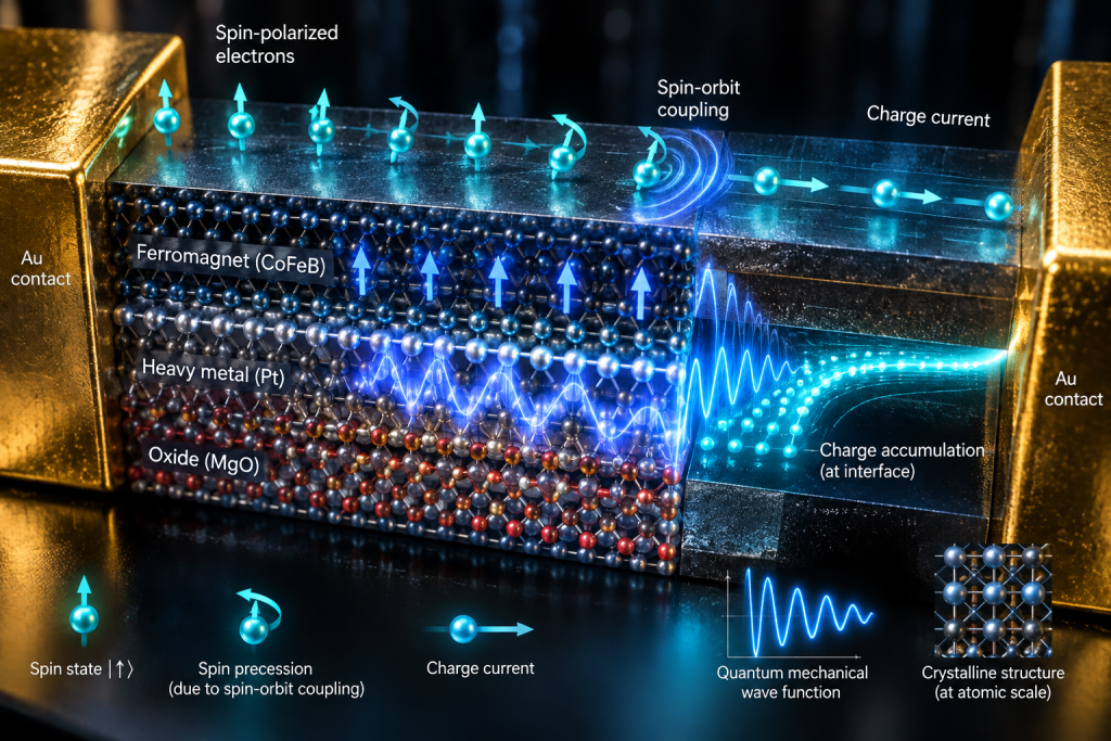
Image generated by AI
Imagine if you could harvest electricity not just from moving electrons, but from the intrinsic spinning motion of those electrons themselves. That’s essentially what spin-to-charge conversion does—it transforms the quantum mechanical “spin” of electrons into usable electrical current. For decades, physicists treated spin as little more than an interesting curiosity, a quantum property with no practical use. Today, this phenomenon is reshaping electronics, promising computers that consume less power and memories that never forget.
The race to develop spintronic devices has intensified dramatically over the past decade as researchers confront a fundamental challenge: silicon-based electronics are approaching the limits of miniaturization. Spin-to-charge conversion offers a pathway around this bottleneck, enabling entirely new classes of devices that could revolutionize data storage, computing, and sensing. Major technology companies and research institutions worldwide are now investing billions into spintronic research, recognizing that the next generation of efficient computing may depend on mastering this quantum phenomenon.
What Is Spin-to-Charge Conversion and Spintronic Devices?
Spin-to-charge conversion is a physical process that converts the angular momentum of spinning electrons—their intrinsic spin—into measurable electrical signals. In conventional electronics, we care only about the flow of charge; electrons moving from point A to point B carry electric current. But electrons possess another fundamental property: they spin, like tiny tops rotating on their axes. This spin can point “up” or “down” relative to a chosen direction. Remarkably, a pure spin current—where electrons with opposite spins flow in opposite directions, producing no net charge flow—can be converted into a real electrical charge current through specialized materials and geometries. Spintronic devices exploit this conversion to create transistors, memory cells, and sensors with unprecedented efficiency.
The modern era of spintronics began in 1988 when physicists Albert Fert and Peter Grünberg independently discovered giant magnetoresistance (GMR), a phenomenon where the electrical resistance of certain magnetic materials changes dramatically in response to external magnetic fields. This discovery earned them the Nobel Prize in Physics in 2007 and immediately suggested practical applications in data storage and magnetic sensors. Throughout the 1990s and 2000s, researchers developed increasingly sophisticated spintronic devices, including spin-valve transistors and magnetic tunnel junctions. However, the integration of spin currents into conventional silicon electronics remained challenging until the discovery of spin Hall effect and inverse spin Hall effect, which enabled efficient spin-to-charge and charge-to-spin conversions at room temperature without requiring magnetic materials.
The Basic Principle
To understand spin-to-charge conversion, we must first grasp what spin actually is. In quantum mechanics, spin is an intrinsic form of angular momentum that has no classical analogue—it’s not that electrons are actually spinning like tiny balls. Rather, it’s a quantum property that manifests as a magnetic moment and behaves as if it were angular momentum. Each electron’s spin can be measured as either “spin-up” or “spin-down” along any chosen axis. The remarkable insight of spintronics is that we can separate the flow of spin-up and spin-down electrons, creating a “spin current” where charge is conserved but spin angular momentum flows. When this spin current encounters certain materials with strong spin-orbit coupling—a quantum mechanical effect where an electron’s orbital motion and spin are intertwined—the spin current converts into a charge current via the inverse spin Hall effect.
Here’s a useful analogy: imagine two rivers flowing side-by-side in opposite directions, one carrying passengers traveling north, the other carrying passengers traveling south. Individually, each river carries no net flow of people. Now imagine a bridge that selectively converts northbound travelers into eastbound travelers and southbound travelers into westbound travelers. Suddenly, you’ve created a net flow of people in the east-west direction from two opposing north-south flows. This is essentially what happens at a spin Hall material interface: the “northbound” and “southbound” spin-up and spin-down electrons get converted into a net flow of charge in a perpendicular direction. The efficiency of this conversion depends on the strength of spin-orbit coupling in the material and the quality of the interface between materials.
Why It Matters in the Real World
Spin-to-charge conversion is crucial for modern electronics because it enables energy-efficient devices with novel functionality. Traditional transistors dissipate energy as heat because they rely on moving charges against resistance. Spintronic devices can operate at much lower voltages and currents, generating less waste heat while performing the same computational tasks. This efficiency gain is increasingly important as data centers consume ever-larger portions of global electricity production. Moreover, spintronic memory devices can retain information without continuous power, unlike traditional RAM, potentially revolutionizing data storage and computing architecture. Research indicates that widespread adoption of spintronic devices could reduce the energy consumption of information technology by 10-20%, with profound implications for climate change and sustainability.
Currently, the most developed commercial application of spintronic principles is in read heads for hard disk drives, where giant magnetoresistance and tunnel magnetoresistance sensors have been standard for over two decades. Magnetic random-access memory (MRAM) using spin-to-charge conversion principles is now being manufactured by companies like Everspin and STMicroelectronics, offering non-volatile storage that combines the speed of conventional RAM with the permanence of disk storage. Emerging applications include spin Hall effect sensors for detecting magnetic fields in automotive systems, medical imaging devices, and precision navigation. Research laboratories are actively developing all-spintronic transistors and logic gates that could eventually replace conventional silicon transistors, particularly in low-power, Internet-of-Things applications.
Recent Breakthroughs in Spin-to-Charge Conversion and Spintronic Devices
The past three years have witnessed remarkable progress in spintronic device efficiency and reliability. In 2022-2023, researchers at institutions including MIT, Stanford, and the Max Planck Institute achieved spin Hall conversion efficiencies exceeding 50% in engineered heterostructures—essentially matching the theoretical predictions from a decade earlier. Scientists have demonstrated that carefully engineering the interface between different materials can dramatically enhance spin-to-charge conversion by optimizing the crystalline structure and chemical composition. Additionally, researchers discovered new materials with exceptionally strong spin-orbit coupling, including topological materials and transition metal dichalcogenides, which promise even higher conversion efficiencies. These advances bring practical, room-temperature spintronic devices significantly closer to commercial viability.
Current research frontiers include developing spintronic devices that operate at room temperature without external magnetic fields, engineering materials with tunable spin-orbit coupling for device optimization, and integrating spintronic elements seamlessly with existing silicon electronics. Teams worldwide are investigating the fundamental limits of spin-to-charge conversion efficiency, exploring whether quantum mechanical effects like quantum Hall phenomena can further enhance conversion. Another active area involves developing spintronic neurons and synapses for neuromorphic computing—using spintronic principles to create artificial brain-inspired hardware that could revolutionize artificial intelligence and machine learning. These open questions will likely dominate the field for the next 5-10 years.
Why Spin-to-Charge Conversion and Spintronic Devices Matters for the Future
As we approach physical limits on traditional silicon transistor miniaturization, spintronic devices represent a genuinely transformative technology pathway. The Information and Semiconductor Industry Association projects that by 2030, spintronic devices could occupy a 10-15% share of the memory and sensor markets, with potential to grow substantially thereafter. Spintronic technology aligns with global sustainability goals by dramatically reducing power consumption in computing and data processing. Beyond efficiency, spintronics enables entirely new computing paradigms, including quantum-inspired probabilistic computing and neuromorphic architectures that more closely mimic biological brains. Governments and multinational corporations recognize this potential: the European Union’s Horizon 2020 program allocated over €100 million to spintronic research, while major tech firms have established dedicated spintronic research divisions.
However, significant challenges remain before spintronics can fully replace conventional electronics. Spintronic devices currently operate at higher voltages than theoretical predictions suggest, indicating that interface engineering and material quality must improve substantially. Integrating spintronic elements with existing semiconductor fabrication infrastructure requires solving complex manufacturing challenges. Additionally, the sensitivity of spintronic devices to magnetic noise and thermal fluctuations requires sophisticated shielding and error correction schemes. Fundamental questions about quantum decoherence in spintronic systems—how quickly spin information is lost—remain only partially answered. These obstacles are formidable but not insurmountable, and the sustained research effort suggests solutions are achievable within the next decade.
Key Takeaways
- Spin-to-charge conversion transforms the quantum spin of electrons into measurable electrical current through interactions with materials possessing strong spin-orbit coupling.
- The inverse spin Hall effect is the primary mechanism enabling practical spin-to-charge conversion, where pure spin currents are converted into charge currents at material interfaces.
- Spintronic memory devices like MRAM offer non-volatile storage combining the speed of conventional RAM with permanent data retention, already achieving commercial deployment.
- Recent breakthroughs have achieved spin Hall conversion efficiencies exceeding 50%, bringing room-temperature, magnetic-field-free spintronic devices closer to practical deployment.
- Widespread adoption of spin-to-charge conversion technology could reduce information technology energy consumption by 10-20%, with profound implications for sustainable computing and artificial intelligence applications.
Explore TED Talks on Spin-to-Charge Conversion and Spintronic Devices:
TED content is used under CC BY-NC-ND 4.0. © TED Conferences, LLC.
Frequently Asked Questions
How does electron spin differ from the charge that conventional electronics rely on?
Electron spin is an intrinsic quantum mechanical property representing angular momentum, independent of the electron's physical motion or charge. While conventional electronics manipulate electron flow (charge movement), spin-to-charge conversion exploits this separate quantum property to generate electrical signals without requiring charge displacement.
What is the physical mechanism that converts spin angular momentum into electrical current?
Spin-to-charge conversion typically occurs through phenomena like the inverse spin Hall effect, where a spin current traveling through a material with strong spin-orbit coupling is transformed into a detectable charge current perpendicular to both the spin direction and current flow. This conversion relies on the interaction between electron spin and the material's crystal lattice properties.
Why does spin-to-charge conversion offer an advantage over silicon-based electronics as devices become smaller?
Silicon-based electronics face miniaturization limits due to heat dissipation and quantum tunneling effects at smaller scales, whereas spintronic devices can encode and manipulate information using spin orientation rather than charge alone, potentially reducing power consumption and enabling operation at smaller dimensions. This makes spin-based systems more energy-efficient and scalable beyond conventional silicon constraints.
Can spin information be preserved and manipulated in practical materials at room temperature?
Yes, recent advances have demonstrated spin coherence and manipulation in various materials at room temperature, though maintaining spin information remains challenging compared to charge-based systems due to spin decoherence from environmental interactions. Researchers are developing materials with enhanced spin-orbit coupling and reduced decoherence rates to make room-temperature spintronic devices viable.